- 您现在的位置:买卖IC网 > Sheet目录527 > SUP75N03-04-E3 (Vishay Siliconix)MOSFET N-CH D-S 30V TO220AB
SUP/SUB75N03-04
Vishay Siliconix
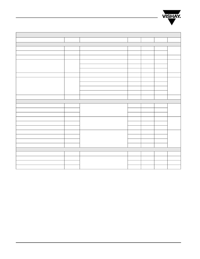
SPECIFICATIONS T J = 25 °C, unless otherwise noted
Parameter
Symbol
Test Conditions
Min
Typ a
Max
Unit
Static
Drain-Source Breakdown Voltage
Gate Threshold Voltage
Gate-Body Leakage
V (BR)DSS
V GS(th)
I GSS
V GS = 0 V, I D = 250 μA
V DS = V GS , I D = 250 μA
V DS = 0 V, V GS = ± 20 V
30
1
3
± 500
V
nA
V DS = 30 V, V GS = 0 V
1
Zero Gate Voltage Drain Current
I DSS
V DS = 30 V, V GS = 0 V, T J = 125 °C
50
μA
V DS = 30 V, V GS = 0 V, T J = 175 °C
200
On-State Drain Current b
I D(on)
V DS = 5 V, V GS = 10 V
V GS = 10 V, I D = 75 A
120
0.0034
0.004
A
Drain-Source On-State Resistance b
r DS(on)
V GS = 4.5 V, I D = 75 A
V GS = 10 V, I D = 25 A, T J = 125 °C
0.005
0.006
0.006
Ω
V GS = 10 V, I D = 25 A, T J = 175 °C
0.008
Forward
Transconductance b
g fs
V DS = 15 V, I D = 25 A
30
S
Dynamic
Input Capacitance
C iss
10742
Output Capacitance
Reverse Transfer Capacitance
Total Gate Charge
Gate-Source Charge
Gate-Drain Charge
Turn-On Delay Time
Rise Time
Turn-Off Delay Time
Fall Time
C oss
C rss
Q g
Q gs
Q gd
t d(on)
t r
t d(off)
t f
V GS = 0 V, V DS = 25 V, f = 1 MHz
V DS = 30 V, V GS = 10 V, I D = 75 A
V DD = 30 V, R L = 0.6 Ω
I D ? 50 A, V GEN = 10 V, R G = 2.5 Ω
1811
775
200
40
40
20
40
190
95
250
40
pF
nC
ns
Source-Drain Diode Ratings and Characteristics
Diode Forward Voltage b
Reverse Recovery Time
V SD
t rr
I F = 75 A, V GS = 0 V
70
1.3
120
V
ns
Peak Reverse Recovery Current
Reverse Recovery Charge
I RM(rec)
Q rr
I F = 50 A, di/dt = 100 A/μs
2.8
0.1
6
0.36
A
μC
Notes:
a. For design aid only; not subject to production testing.
b. Pulse test; pulse width ≤ 300 μs, duty cycle ≤ 2 %.
Stresses beyond those listed under “Absolute Maximum Ratings” may cause permanent damage to the device. These are stress ratings only, and functional operation
of the device at these or any other conditions beyond those indicated in the operational sections of the specifications is not implied. Exposure to absolute maximum
rating conditions for extended periods may affect device reliability.
www.vishay.com
2
Document Number: 70745
S-62484-Rev. F, 04-Dec-06
发布紧急采购,3分钟左右您将得到回复。
相关PDF资料
SUP75P03-07-E3
MOSFET P-CH D-S 30V TO220AB
SUP90N08-7M7P-E3
MOSFET N-CH D-S 75V TO220AB
SUP90P06-09L-E3
MOSFET P-CH 60V 90A TO220AB
SUV85N10-10-E3
MOSFET N-CH D-S 100V TO220AB
SV-LED-125E
HEATSINK DEGREASED 25.4MM
SV21C201BJA01B00
ROTARY POS SENSOR 200 DEGREE
SX1210I084T
IC SINGLE-CHIP RECEIVER 32-TQFN
SX1211SK915
KIT STARTER FOR SX1211 915MHZ
相关代理商/技术参数
SUP75N03-07
功能描述:MOSFET 30V 75A 120W RoHS:否 制造商:STMicroelectronics 晶体管极性:N-Channel 汲极/源极击穿电压:650 V 闸/源击穿电压:25 V 漏极连续电流:130 A 电阻汲极/源极 RDS(导通):0.014 Ohms 配置:Single 最大工作温度: 安装风格:Through Hole 封装 / 箱体:Max247 封装:Tube
SUP75N04-05L
功能描述:MOSFET 40V 75A 130W RoHS:否 制造商:STMicroelectronics 晶体管极性:N-Channel 汲极/源极击穿电压:650 V 闸/源击穿电压:25 V 漏极连续电流:130 A 电阻汲极/源极 RDS(导通):0.014 Ohms 配置:Single 最大工作温度: 安装风格:Through Hole 封装 / 箱体:Max247 封装:Tube
SUP75N04-05L-E3
功能描述:MOSFET 40V 75A 130W RoHS:否 制造商:STMicroelectronics 晶体管极性:N-Channel 汲极/源极击穿电压:650 V 闸/源击穿电压:25 V 漏极连续电流:130 A 电阻汲极/源极 RDS(导通):0.014 Ohms 配置:Single 最大工作温度: 安装风格:Through Hole 封装 / 箱体:Max247 封装:Tube
SUP75N04-05L-T1-E3
制造商:Vishay Intertechnologies 功能描述:N CHANNEL MOSFET, 40V, 75A, TO-263, Transistor Polarity:N Channel, Continuous Dr
SUP75N05-06
功能描述:MOSFET 50V 75A 250W RoHS:否 制造商:STMicroelectronics 晶体管极性:N-Channel 汲极/源极击穿电压:650 V 闸/源击穿电压:25 V 漏极连续电流:130 A 电阻汲极/源极 RDS(导通):0.014 Ohms 配置:Single 最大工作温度: 安装风格:Through Hole 封装 / 箱体:Max247 封装:Tube
SUP75N05-06A
制造商:Vishay Angstrohm 功能描述:Trans MOSFET N-CH 50V 75A 3-Pin(3+Tab) TO-220AB
SUP75N05-06A-E3
功能描述:MOSFET 50V 75A 250W RoHS:否 制造商:STMicroelectronics 晶体管极性:N-Channel 汲极/源极击穿电压:650 V 闸/源击穿电压:25 V 漏极连续电流:130 A 电阻汲极/源极 RDS(导通):0.014 Ohms 配置:Single 最大工作温度: 安装风格:Through Hole 封装 / 箱体:Max247 封装:Tube
SUP75N05-06-E3
功能描述:MOSFET 50V 75A 250W RoHS:否 制造商:STMicroelectronics 晶体管极性:N-Channel 汲极/源极击穿电压:650 V 闸/源击穿电压:25 V 漏极连续电流:130 A 电阻汲极/源极 RDS(导通):0.014 Ohms 配置:Single 最大工作温度: 安装风格:Through Hole 封装 / 箱体:Max247 封装:Tube
